Mastering PCB Design and Analysis with OrCAD: A Comprehensive Guide
Introduction: Printed Circuit Boards (PCBs) are essential components in electronic devices, serving as the foundation for interconnecting electronic components and providing electrical pathways for signal transmission. Designing and analyzing PCBs require specialized software tools capable of handling complex layouts, routing requirements, and electrical considerations. OrCAD is a leading software suite developed by Cadence Design Systems for PCB design, simulation, and analysis. In this comprehensive guide, we will explore the intricacies of using OrCAD for PCB design and analysis, covering everything from schematic capture to layout routing and signal integrity analysis.
Section 1: Understanding PCB Design with OrCAD
1.1 Overview of PCB Design: PCB design involves the creation of schematics, placement of components, routing of traces, and generation of manufacturing files for fabrication. OrCAD provides a comprehensive platform for designing PCBs, offering tools for schematic capture, component management, layout routing, and design rule checking (DRC) to ensure manufacturability and reliability.
1.2 Importance of PCB Design: PCB design is crucial for ensuring the functionality, performance, and reliability of electronic devices. Well-designed PCBs optimize signal integrity, minimize electromagnetic interference (EMI), and simplify assembly and testing processes, ultimately reducing time-to-market and production costs for electronic products.
1.3 Role of OrCAD: OrCAD plays a vital role in PCB design by providing engineers and designers with intuitive tools, advanced features, and comprehensive workflows for designing, simulating, and analyzing electronic circuits. With its user-friendly interface, extensive libraries, and powerful simulation capabilities, OrCAD streamlines the PCB design process and empowers users to create high-quality, manufacturable PCB layouts.
Section 2: Introduction to OrCAD Software Suite
2.1 Overview of OrCAD: OrCAD is a suite of software tools developed by Cadence Design Systems for electronic design automation (EDA), including schematic capture, PCB layout, simulation, and analysis. It offers a range of modules and packages tailored to specific design tasks, such as OrCAD Capture for schematic design, OrCAD PCB Editor for layout routing, and OrCAD PSpice for circuit simulation.
2.2 OrCAD Features and Capabilities: OrCAD provides a wide range of features and capabilities for PCB design and analysis, including:
- Schematic capture: Create hierarchical schematics, symbol libraries, and component footprints for electronic circuits.
- PCB layout: Place components, route traces, define copper pours, and generate manufacturing outputs for PCB fabrication.
- Simulation: Perform circuit simulation, signal integrity analysis, and electromagnetic compatibility (EMC) analysis to validate design performance.
- Design rule checking (DRC): Verify design compliance with electrical, mechanical, and manufacturability constraints to ensure design integrity and reliability.
2.3 Benefits of Using OrCAD: OrCAD offers several benefits for engineers and designers involved in PCB design, including:
- Streamlined design process: Intuitive user interface, customizable workflows, and automation features accelerate design iteration and reduce time-to-market.
- Comprehensive analysis capabilities: Built-in simulation tools, signal integrity analysis, and design rule checking ensure design reliability and performance.
- Seamless integration: Integration with other EDA tools, mechanical CAD software, and manufacturing platforms enables seamless data exchange and collaboration throughout the design cycle.
Section 3: PCB Design Workflow with OrCAD
3.1 Schematic Capture: Engineers begin the PCB design process by creating schematics using OrCAD Capture. They place components, connect nets, and define design constraints to capture the electrical connectivity and functional relationships of the circuit.
3.2 Component Management: OrCAD provides extensive component libraries and management tools for selecting, placing, and customizing electronic components. Engineers can search libraries, import vendor data, and create custom components to populate schematics and layouts accurately.
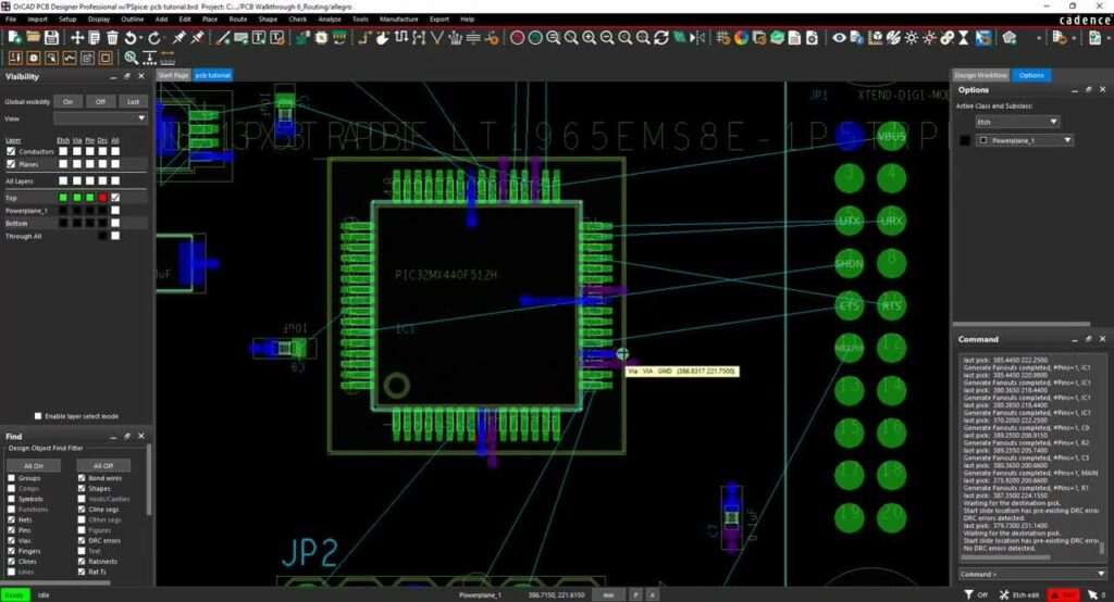
3.3 Layout Routing: OrCAD PCB Editor enables engineers to translate schematics into physical PCB layouts by placing components and routing traces on the PCB substrate. They use manual routing, automated routing, and interactive routing tools to optimize signal paths, minimize crosstalk, and meet design constraints.
3.4 Design Rule Checking (DRC): OrCAD performs design rule checking (DRC) to verify design compliance with electrical, mechanical, and manufacturability constraints. Engineers define design rules for trace width, clearance, spacing, via placement, and manufacturing tolerances to ensure design integrity and reliability.
3.5 Manufacturing Outputs: OrCAD generates manufacturing outputs, including Gerber files, NC drill files, assembly drawings, and bill of materials (BOM), for PCB fabrication and assembly. Engineers review outputs, perform design reviews, and collaborate with manufacturing partners to ensure successful production of PCBs.
Section 4: PCB Analysis and Simulation with OrCAD
4.1 Circuit Simulation: OrCAD PSpice provides engineers with powerful simulation capabilities for analyzing circuit behavior, performance, and reliability. They simulate electrical circuits, verify design functionality, and optimize component values to meet design specifications and performance requirements.
4.2 Signal Integrity Analysis: OrCAD Signal Integrity analyzes high-speed digital signals, differential pairs, and transmission lines to predict signal integrity issues such as reflections, crosstalk, and timing violations. Engineers perform pre-layout and post-layout analysis to optimize signal integrity and minimize signal degradation in PCB designs.
4.3 Electromagnetic Compatibility (EMC) Analysis: OrCAD EMC analyzes electromagnetic interference (EMI) and electromagnetic compatibility (EMC) issues in PCB designs to ensure compliance with regulatory standards and industry guidelines. Engineers assess radiated emissions, conducted emissions, and susceptibility levels to identify potential sources of interference and mitigate EMI risks.
Section 5: Advanced Techniques and Optimization Strategies
5.1 High-Speed Design: Engineers apply high-speed design techniques and optimization strategies to address signal integrity challenges in high-speed PCB designs. They use controlled impedance routing, differential pair routing, length matching, and termination techniques to minimize signal distortion and maintain signal integrity in high-speed signaling environments.
5.2 Thermal Management: OrCAD supports thermal analysis and optimization of PCB designs to manage heat dissipation and ensure reliable operation of electronic components. Engineers perform thermal simulations, analyze thermal profiles, and optimize copper pours, component placement, and heatsink design to prevent thermal issues and thermal-induced failures.
5.3 Design for Manufacturability (DFM): Engineers consider manufacturability constraints and guidelines during PCB design to facilitate smooth production and assembly processes. They optimize design layouts, panelization, fiducial placement, and solder mask configurations to minimize manufacturing defects, improve yield rates, and reduce production costs.
Section 6: Best Practices and Tips for OrCAD PCB Design
6.1 Collaboration and Communication: Foster collaboration and communication among design teams, stakeholders, and manufacturing partners throughout the PCB design process. Use OrCAD’s collaboration features, version control tools, and design review capabilities to facilitate feedback, resolve issues, and ensure alignment with project goals and objectives.
6.2 Design Validation and Verification: Validate and verify PCB designs using simulation, analysis, and prototyping techniques to ensure design integrity and reliability. Conduct design reviews, simulations, and test validations to identify and address potential issues early in the design cycle and minimize rework and redesign efforts.
6.3 Continuous Learning and Improvement: Stay updated on the latest developments, advancements, and best practices in PCB design and technology. Participate in training programs, workshops, and industry events to enhance proficiency in OrCAD software, learn new techniques, and explore emerging trends in PCB design and electronics manufacturing.
Conclusion: Using OrCAD for PCB design and analysis provides engineers and designers with a comprehensive toolset for creating high-quality, reliable, and manufacturable printed circuit boards. By mastering the principles, techniques, and best practices discussed in this guide, engineers can leverage OrCAD to streamline the design process, optimize design performance, and achieve excellence in PCB design and engineering. With its advanced features, comprehensive workflows, and seamless integration, OrCAD continues to be a trusted platform for PCB design and analysis in industries ranging from electronics and telecommunications to automotive and aerospace, empowering users to innovate and succeed in a rapidly evolving technological landscape.